|
The Clock/Timing Board
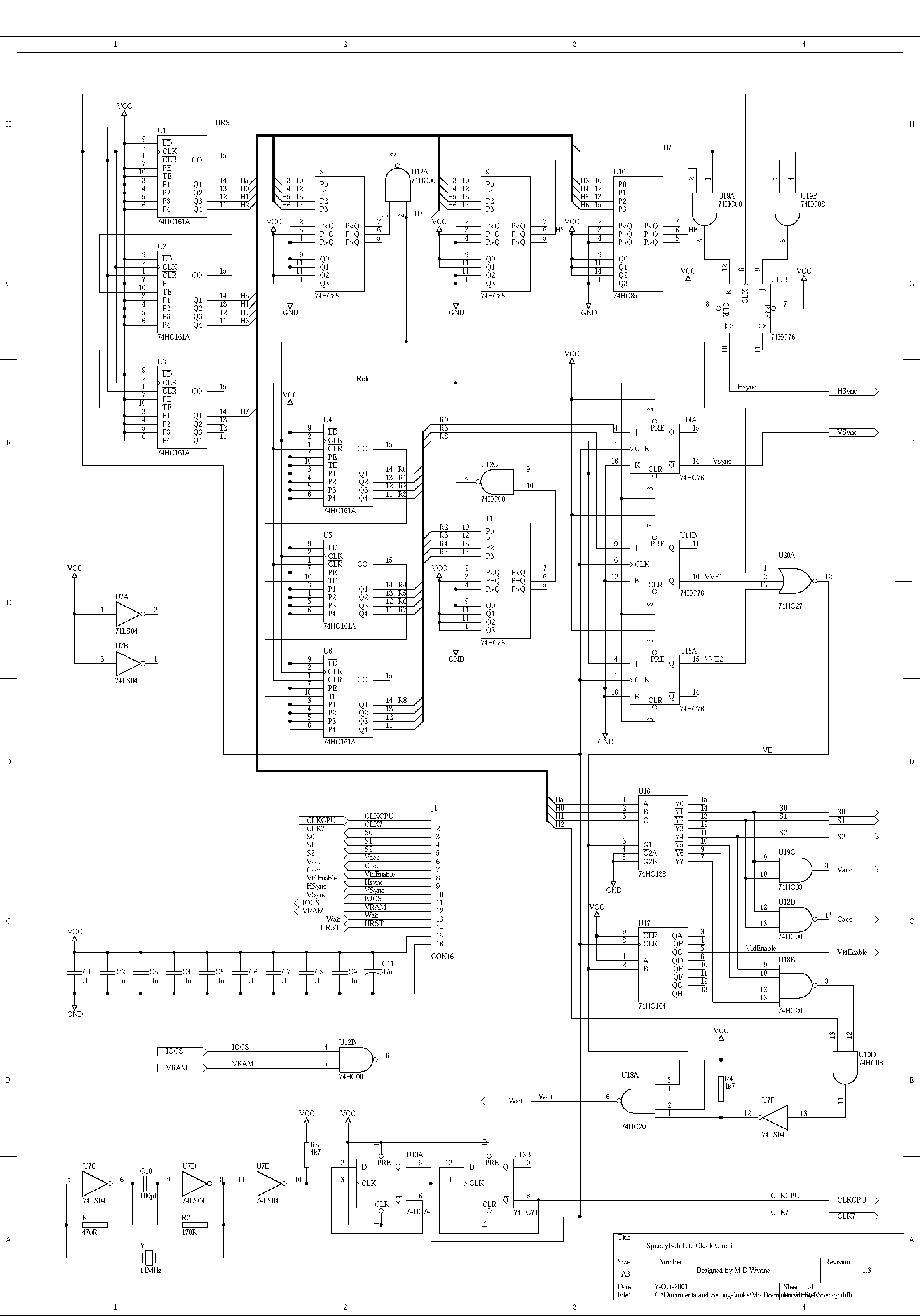
OK, I hope someone can understand this... U7C,D & E along with the crystal form a 14Mhz clock which is divided by 2, then by 2 again by U13 to create the 7Mhz and 3.5Mhz clocks. U1,2 & 3 (4 bit synchronous counters) are clocked at 7MHz. U8 along with U12a detect when the counter has counted to 448 and reset, thus forming a modulo-448 counter. This forms the length of the horizontal scanline (448 is 224 T-states * 2 because the counter is clocked at 7MHz, not 3.5). H7 from this counter is used as an active low Horizontal display enable (Low for the first 256 counts, then high). U9 & U10 pick out the start and end of the Horizontal Sync pulse which gets latched by U15B. U4, 5 & 6 form the vertical counter. They are clocked by H7 of the horizontal counter so that they count scanlines. U11 with U12C reset the counter when it reached 312 so that 312 scanlines are produced on the monitor. U14A latches the Vertical Sync pulse. It is cleared whenever the vertical counter is reset, then set again at the end of the first line (R0 goes high). U14B signals the end of the top border. Like the Vertical sync pulse it is cleared then the counter is reset, but sets on R6 (line 64). U15A marks the start of the bottom border. It is reset on with the counter and set with R8 (line 256). The area between line 64 and 256 marks the displayable area. The above 2 signals, along with the horizontal video enable are then NOR'd together to produce the Video Enable line. The clock board is also responsible for synchronising the activities of the video board. To do this, as well as using VE (Video Enable), it can send 5 signals to the video circuitry: S0, S1, S2, Vacc & Cacc. These signals are derrived from the Horizontal counter by U16 (a 3 to 8 line decoder). S0 tells the video circuit to load the attribute byte from RAM. S1 signifies that the bitmap should be loaded from RAM, and also starts the output of a new byte. S2 tells the video board to increment its address counter. Vacc and Cacc are responsible for deciding whether the CPU or video circuitry have access to Video RAM. Vacc is active on states S0 & S1, Cacc at all other times. U16 along with U18 also control contended RAM timing. If IOCS (a ULA IO access) or VRAM (A video RAM access) is enabled, the Z80 is paused 'till it is allowed access again. Finally, U17 delays the Video Enable
line to the video board until after the the first attribute is fetched
from RAM and the bitmap is ready to be displayed.
|
Site designed and hosted by Mike Wynne